System Configuration
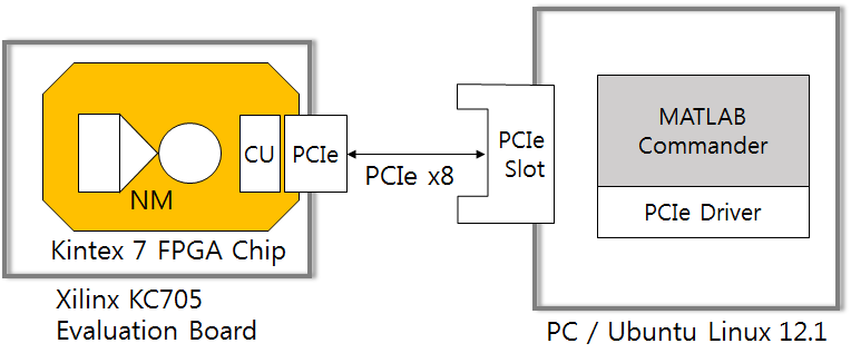
The system designed on the Matlab hardware simulator was ported on a Xilinx KC705 FPGA board. The original FPGA implementation described in the paper has revised thereafter. Following figure shows the revised configuration of the FPGA system.
Xilinx KC705 board contains a Xilinx Kintex 7 FPGA chip. On the FPGA chip, an NM system with an x8 PCIe block was implemented. The board is plugged into the PCIe slot of a PC with Ubuntu Linux OS. In the PC, Matlab software communicates with the NM using PCIe device driver. The Matlab setups the systems parameters, initializes block memories in the NM system, monitors the system, and displays the computation results. The Kintex 7 FPGA chip (xc7k325) is a mid-range chip between Virtex 7 (high-end) and Artix 7 (low-end) in the Xilinx FPGA products.
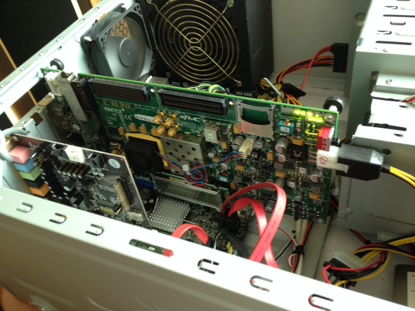
Following figure shows the picture of the system.
Configuration of the NM system
The design of the NM system has modified to fit in the FPGA chip. The configuration of the system is shown as following.
- DBN size : 784 x 96 x 96 x 448
- Connection weight and neuron state representation : 32-bit
- Arithmetic operation : single-precision floating-point
- Number of neuron machine on the chip : 1
- Number of SNUs (P) : 32
- System clock : 250 MHz
In this implementation, single-precision floating point (FP) arithmetic operator IPs are used throughout the system. Pipeline delays of multipliers, adders, exponent FP operators are 6, 9, and 20 clock cycles, respectively. In addition, a linear-feedback-shift-registers (LFSR) circuit is used to generate random numbers. Note that the DBN size (and network topology) is not fixed by hardware. It can be changed by commands from the PC without changing hardware.
In the previous FPGA implementations for other neural models, we used a Microblaze processor for communication between PC and the NM system for management purpose, and the processor slowed down the communication link. In this implementation, we removed the processor from the design and the communication is carried out directly between the PC and NM system via PCIe interface. Thereby, our implementation became truly a processor-less design.
PC-FPGA Interface
As stated above, Matlab software in PC side controls the NM system. Most system global parameters, such as learning rates, network topologies, initial weights can be set using it. The result of the computation, such as current time step, mean square errors, trained weights, can be read from the NM system and displayed on the screen. Please note that although we used MATLAB programs in many ways (for hardware simulator and hardware controller), none of them is for actual neural computation. They are used as utility programs.
Place-and-route result
The design was successfully synthesized and place-and-routed without timing error as shown in the following figure.
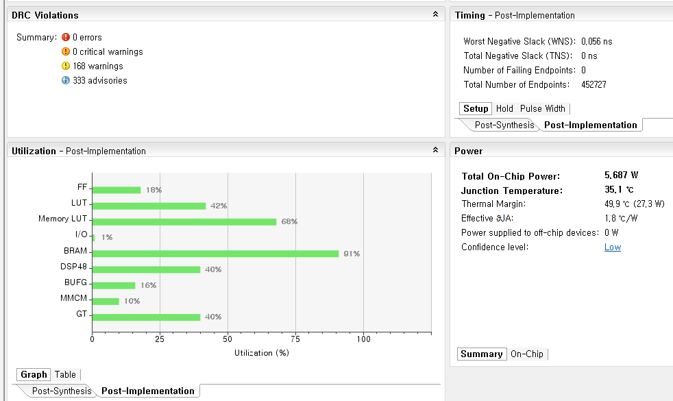
The display of Xilinx Vivado tool after place and route, showning compile status, timing, resource utilization summary, and on-chip power consumption
As shown in the figure, 42 % of total LUTs, 40 % of DSP slices, and 91 % of block RAM was utilized to build the system. Total on-chip power consumption was reported as 5.687 watts.
Fidelity analysis
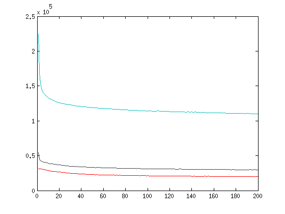
We ran 200 epochs each with 60000 MNIST training data and obtained the following MSE trace.
MSEs of the first, second, and third RBM layers are shown in blue, black, and red.
Proportion of FP operators
As combinations of LUTs and DSP slices were used to implement FP operators for the FPGA system, it was hard to figure out the resource proportions. Therefore we recompiled the system without using DSP slices to calculate the proportion of the FP operators more clearly. Total resources used for the system in this case, the resources used for FP operators, and the proportion of the FP operators are shown in the following table.
In conclusion, the proportion of resources used for FP operators is approximately 73%. Only 27% are used for other logic components including PCI-e interface, pipeline registers, and so forth (excluding memories). A detailed resource report of our implementation can be downloaded from here.
Computational speed
The speed of the system was checked by monitoring the time spent for each epochs. It took approximately 3.582 seconds for each 60000-train-data epoch, as the controller program reported.
...

Elapsed time is 3.581610 seconds.

Elapsed time is 3.581732 seconds.

Elapsed time is 3.581802 seconds.

Elapsed time is 3.581696 seconds.

Elapsed time is 3.581638 seconds.

...
As 127488 connection weights (784×96 + 96×96 + 96×448) are trained for each train data, 7.65 x 10^9 connections are updated in each 60000-train-data epoch. Therefore the computational speed of our implementation is 7.65 x 10^9 / 3.582 = 2.136 GCUPS (giga connection updates per second).
Speed comparison
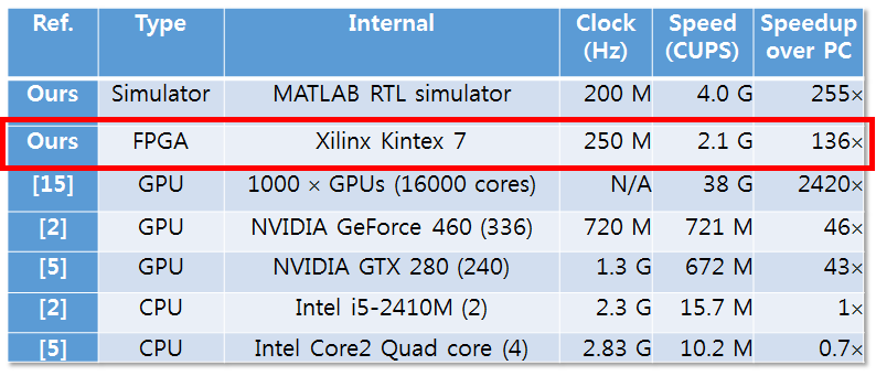
Following table compares the speed of our implementation with other known systems.
As shown in this table, our system exhibited better performance compared to PCs and even GPUs. Note that our system used only a small portion of hardware resources in the mid-range FPGA chip, with small power consumption. Also note that as FPGAs are general purpose hardware with their own overheads (gates being implemented by LUTs), even better performance could be achieved on custom chips (ASICs) using the same computational resources.
